
AIM Photonics Announces New Opto-electronic Testing Services
Comprehensive toolset expands access to companies of all sizes to advanced PIC testing capabilities for their prototype development
AIM Photonics recently announced the launch of its new Opto-electronic Testing Services, featuring a full suite of advanced tools for testing both photonic integrated circuits (PICs) as well as conventional electronic ICs.
The new service will be offered through AIM Photonics’ Test, Assembly and Packaging facility in Rochester, NY, the only place in the U.S. that provides access to both photonic and electronic test, assembly, and packaging prototyping services for substrates up to 300 mm wafers.
“Our comprehensive toolset can test and measure multiple performance aspects of electronic and photonic devices before and immediately after package assembly, allowing for rapid verification and optimization of the manufacturing process all in the same R&D center, saving our members and customers valuable time and resources,” said Chris Striemer, Business Development and Facilities Manager at AIM Photonics test, assembly and packaging facility.
AIM Photonics’ advanced Opto-electronic Testing Services currently includes over 30 tools for passive optical, active optoelectronic, telecom/datacom, and RF and DC testing.
“Providing access to these services is core to our mission to expand the silicon photonics ecosystem,” Striemer said. “With this toolset, we are able offer a wide range of testing capabilities for on-wafer, die-level, and packaged devices, all aimed at achieving consistent and reliable results to support our members’ and customers’ prototype development.”
Striemer also added that the funds recently authorized through Empire State Development by the NYS Photonics Board will further expand AIM Photonics’ test and measurement capabilities over the next several years through additional hardware and partnerships with Rochester area colleges and universities.
“Our customers include not only small businesses, academics and, of course, our government partners, but also research and development groups in companies—both large and small—that want to explore photonics without having to invest in testing infrastructure,” said Amit Dikshit, design enablement manager at AIM Photonics.
Purchasing advanced test and measurement tools can be cost-prohibitive for many companies, particularly start-ups with limited resources, Dikshit added. “Even basic test capability could cost several hundred thousand dollars and take up to a year to purchase, install and test,” he said.
“Having access to our extensive testing capabilities—as well as our finely-tuned methodologies—allows our members and customers to leave the testing to us, freeing them to focus their efforts on designing and developing their own innovative devices and technologies,” Dikshit said.
For more information, contact info@aimphotonics.com.
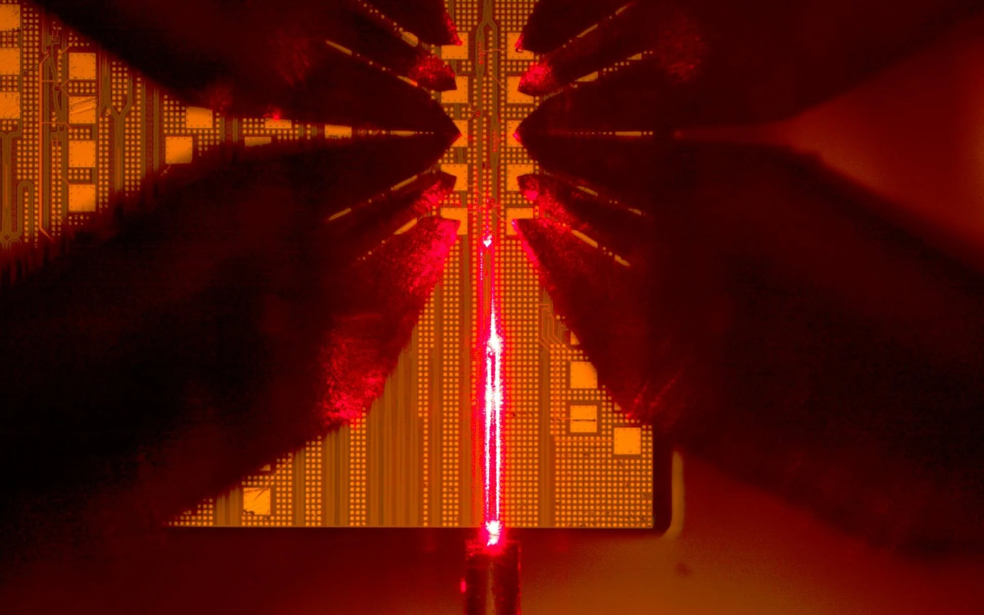
Die-level edge-coupling based electro-optic measurements

The large automated prober in AIM Photonics’ test lab enables programmable optical, DC and RF interrogation of wafer substrates as large as 300 mm, with additional flexibility for die-level testing.

An eye-diagram measured on a photonic integrated circuit is used to evaluate high-speed data quality.