Students Expand their PIC Knowledge and Skills during 3-day Hands-on Photonics Bootcamp
About a dozen students enrolled in STEM programs at U.S. colleges and universities, as well as engineers and designers from both start-ups and established companies in the integrated photonics industry, gathered recently at MIT and BSU with the same goal in mind: to gain more hands-on experience using the schools’ state-of-the art tools to help them better understand photonic integrated circuit (PIC) theory, testing and packaging during AIM Photonics’ hands-on Photonics Bootcamp.
The bi-annual event, which was held Jan. 10-12 at Massachusetts Institute of Technology (MIT) and Bridgewater State University (BSU), kicked off with opening remarks from Dr. Anu Agarwal, Principal Research Scientist at MIT, followed by a deep dive into integrated photonics with a series of lectures and workshops to prepare attendees for the hands-on testing and packaging training that would follow at the Labs for Education & Application Prototype (LEAP) at MIT and BSU, as well as MIT’s Electronic and Photonic Materials Group Lab and Photonics and Electronics Research Group Lab.
Topics and activities conducted during the opening day included:
An introduction to design and processing principles for waveguide-based passive devices, presented by Prof. J.J. Hu of MIT
A VR simulation workshop on device/tool training, led by Dr. Sajan Saini, IKIM Education Director
Simulation and PIC system modeling/SDL layout, led by Dr. Luis Orbe of Synopsys
OPA systems design for LiDAR sensor and augmented reality display PICs, presented by Prof. Jelena Notaros of MIT
Photonics co-packaging standards and innovative new design paradigms, presented by MIT researchers Drew Weninger and Luigi Ranno
PIC theory and strategies for data acquisition and analysis, presented by Prof. Samuel Serna of BSU
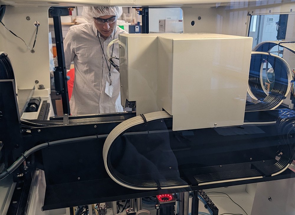
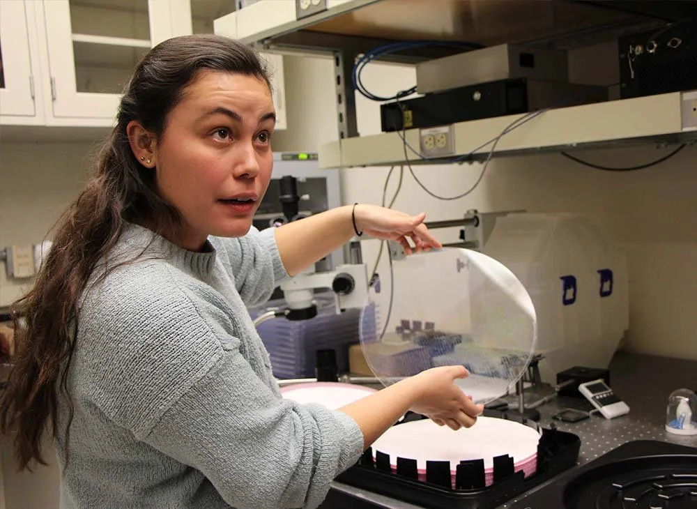
Days 2 and 3 consisted of hands-on lab sessions at MIT and BSU. During these training sessions, which were led by Prof. Samuel Serna, Drew Weninger, Luigi Ranno, Ashton Hattori, Sabrina Corsetti, Pablo Bedoya Rios, and Samuel Bechtold, participants performed a variety of hands-on exercises designed to teach them how to:
couple light into a PIC chip using lensed fibers on six-axis control stages and packaged fiber arrays,
gather and analyze PIC data,
place chips onto a substrate, followed by reflow to create contacts and test the packaged system,
explore free-space optics to better understand fundamental photonics concepts, and
perform non-mechanical beam steering using a PIC chip.
“Overall, it was a very successful event and we are honored to play a key role in the education and workforce development efforts at AIM Photonics as we build a STEM-skilled ecosystem,” Agarwal said.
“The teams at MIT and BSU are highly valued partners in our EWD program,” said Robert Geer, director of Education and Workforce Development at AIM Photonics. “Between the advanced packaging and testing capabilities available at their labs and the deep expertise of our esteemed colleagues at both universities who organize and teach the curriculum, participants in our bootcamps receive a hands-on integrated photonics educational experience unlike anything else offered in the U.S.”
The next Photonics Bootcamp is tentatively scheduled to take place in Fall 2023. More information will be posted on AIM Photonics’ website as planning progresses. Alternatively, you can sign up here to receive email notifications about all of AIM Photonics’ education and workforce development opportunities.