
PIC TESTING AND PACKAGING WORKSHOP
Four days of interactive experiential learning at AIM Photonics’ Test, Assembly and Packaging (TAP) Facility, Rochester Institute of Technology, and the University of Rochester that will teach you how to test, analyze, and package photonic integrated circuits.
DATES: August 4-7, 2026
COURSE TYPE: In-person
LOCATION: Rochester, NY
*Sign up to receive email notifications about this course and other AIM Photonics education and workforce development news
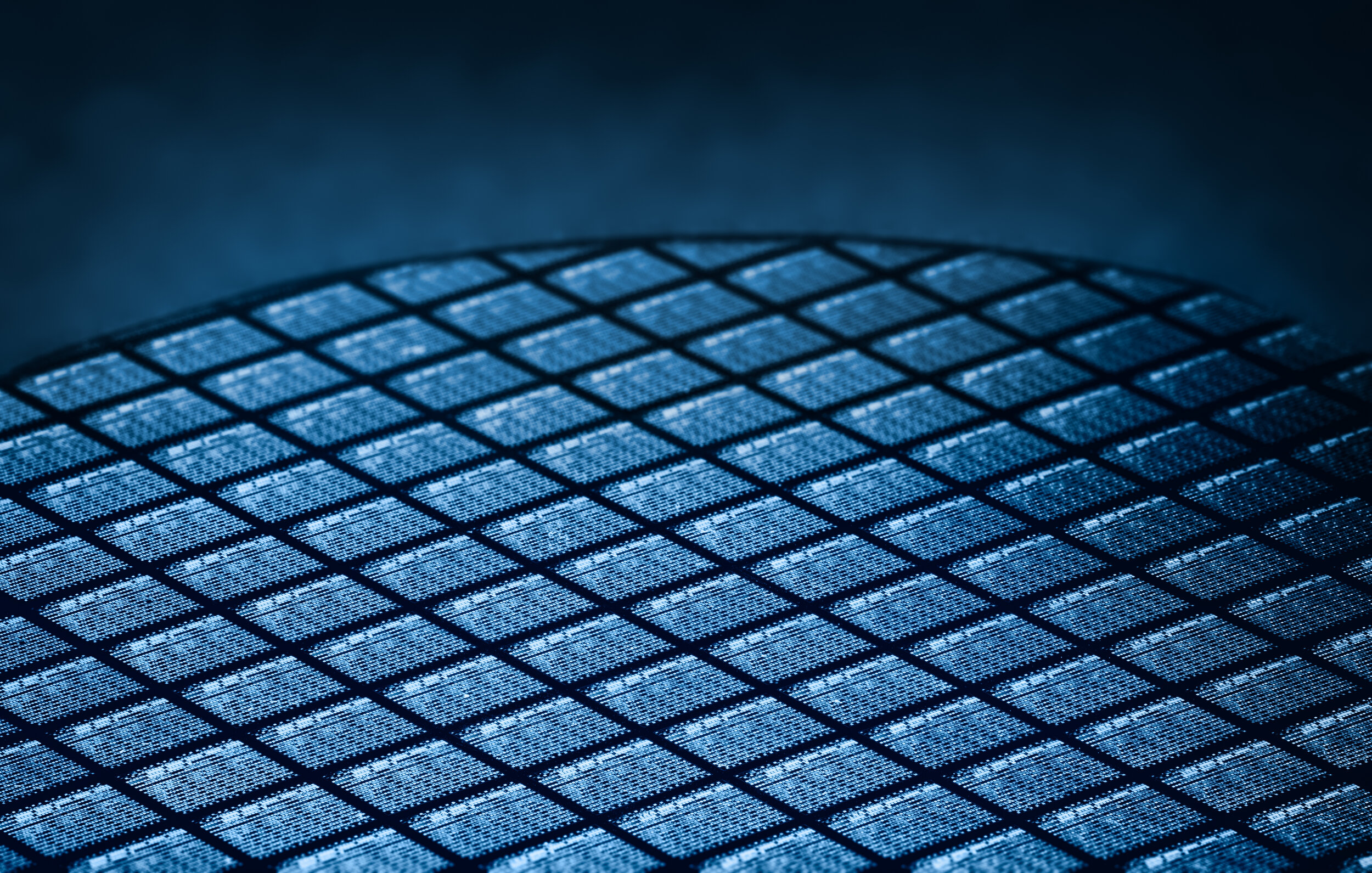
Participants will use the AIM Photonics’ Hands on Photonic Education (HOPE) Datacom Kit, a six-chip photonic integrated chip (PIC) kit focused on the fundamental concepts used in data communications, including:
Insertion Loss
Interference
Mach-Zehnder Modulation
Germanium Photodetectors
Ring Resonator – Wavelength Division Multiplexing (WDM) / Demultiplexing
WDM Micro-ring Modulation
You will learn:
Passive PIC Testing – Coupling/alignment, waveguide loss, and interference
Active PIC Testing – Modulation (Mach-Zehnder and ring resonator) and photodetection
Packaging – Dicing, die bonding, wire bonding, fiber attach (using both traditional and photonic wire bonding technology) and metrology

WHO SHOULD ATTEND?
This workshop is intended for those interested in hands-on and demonstration-based experience in testing and packaging photonic integrated circuits (PICs.) Prior PIC design experience equivalent to the AIM Photonics online course PIC1: Fabless Design of Photonic Integrated Circuits is strongly recommended.
REGISTRATION
Due to overwhelming interest in the PIC Testing and Packaging Workshop (August 4-7, 2026), registration is full. Sign up to receive email updates about upcoming sessions for this course and other AIM Photonics education and workforce development news.
OFAC Registration Guidelines - IMPORTANT
AIM Photonics adheres to the registration guidelines of the United States Office of Foreign Assets and Control (OFAC) sanctions list. U.S. laws and regulations prevent us from allowing persons ordinarily resident in certain countries and regions from participating in the PIC Testing and Packaging Workshop. Consequently, individuals ordinarily resident in Cuba, Iran, North Korea, Syria, and the Crimea region of Ukraine may not register. In addition, persons listed on the Specially Designated Nationals and Blocked Parties list maintained by the U.S. Office of Foreign Assets Control and the Entities List maintained by the U.S. Department of Commerce are prohibited from participating.
Questions?
Contact: Stefan Preble

SCHEDULE-AT-A-GLANCE
Workshop activities will begin at 9 a.m. and end at approximately 5 p.m. each day.
An evening networking event for all workshop participants will be held on Thursday, August 6. More details to come.
| Location | Topics | |
|---|---|---|
| Day 1 | AIM Photonics TAP Facility | • Welcome and Overview • Tour of the TAP facility • Packaging and Testing PICs 101 |
| Days 2 and 3 |
Workshop participants will break into two groups and rotate to spend a full day at each of the following locations: | |
| Rochester Institute of Technology (RIT) | Active PIC testing (Modulators – Mach-Zehnder and resonator), ring resonators (WDM), and packaging using photonic wire bonding | |
| University of Rochester | Loss, interference (directional couplers, Mach-Zehnder interferometers), photodetectors and SWIR chip characterization | |
| Day 4 | AIM Photonics TAP Facility | PIC Packaging Demonstrations: Wafer Dicing, Die Bonding, Wire Bonding, Fiber Array Attachment, Metrology, and Testing |
LOGISTICS
WORKSHOP LOCATIONS
AIM Photonics Test, Assembly and Packaging (TAP) Facility
1964 Lake Avenue, Rochester, NY 14623 (view on Google Maps)
Rochester Institute of Technology (RIT)
IT Collaboratory at the Engineering Building (view on Google Maps)
University of Rochester - Institute of Optics
480 Intercampus Dr. Rochester, NY 14623 (view on Google Maps)
RIT and the University of Rochester are approximately 4 miles away from each other, and approximately 10-13 miles from the TAP facility.
LODGING AND TRANSPORTATION
Attendees must make their own arrangements for lodging and are responsible for their own transport between the three workshop locations. A personal or rental vehicle is strongly recommended. Lyft and Uber are also available.
MATERIALS REQUIRED
Attendees are required to bring a laptop in order to analyze data.

MEET THE INSTRUCTORS
-

STEFAN PREBLE is a professor in the Kate Gleason College of Engineering at the Rochester Institute of Technology. He is an expert in integrated photonic devices and circuits and is working to implement the technology in high-performance computing, communication and sensing systems. Prof. Preble is the lead instructor of the AIM Photonics online course “PIC1: Fabless Design of Photonic Integrated Circuits.”
-

JAIME CARDENAS is currently an assistant professor in The Institute of Optics at the University of Rochester with a secondary appointment at the Department of Physics and Astronomy. His research focuses on novel integrated and nanoscale photonic devices to address scientific and technological challenges in communications, sensing, signal processing, and quantum information science.
-

THOMAS BROWN is professor and director of the Institute of Optics at the University of Rochester. His research focuses on polarized light in free space optics and waveguides, stress engineered optical elements, and the discovery of new metrology methods for photonic integrated circuits.
-
CHRIS STRIEMER is the Business Development and Facilities manager for AIM Photonics’ Test, Assembly and Packaging facility in Rochester, NY, where he coordinates projects with members and customers to most efficiently leverage the institute’s advanced packaging, metrology, and testing capabilities for their prototype designs in order to help drive them toward commercial success.