
WHAT IS INTEGRATED PHOTONICS?
Photonics starts with photons, or particles of light.
According to the insights of quantum physics, light can act as both a wave and a particle – a paradigm first proposed by Albert Einstein in 1905.
Photonics is the science of creating, moving, and detecting photons. It brings together physics, electrical engineering, and materials science knowledge about photons and electrons.
TEDx presentation given by Associate Professor in Chemistry at Stonehill College, Cheryl Schnitzer
Photonics technology surrounds us in the modern world: CT scans, barcodes, LED lights, flatscreen TVS, CD and DVD players, driverless cars, laser-guided missiles, fiber-optic communications, cellular phone networks, solar power, and more. Light-based technologies are efficient, reliable, and fast.
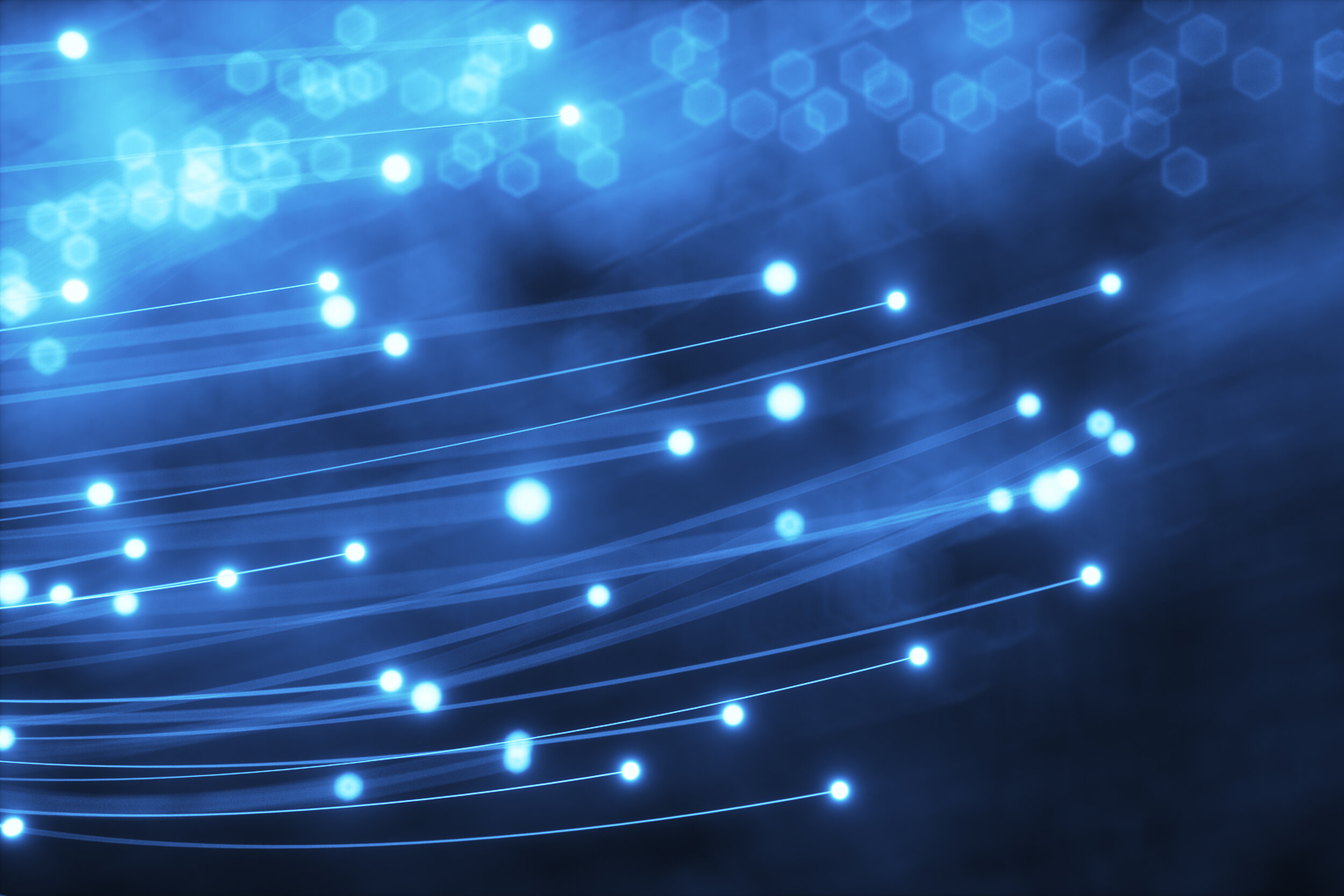
Photonics technology includes sources of light such as lasers and LEDs, waveguides to guide light such as fiber optics, and a variety of opto-electronic devices that encode digital information onto optical signals and convert optical signals to electrical ones. These components are typically discrete and physically separate from one another, and need to be mated together by various coupling means to create a complete optical circuit.
In contrast, integrated photonics is an emerging branch of photonics in which waveguides and devices are fabricated as an integrated structure onto the surface of a flat substrate, or flat surface. As a result of integration, complex photonic circuits can now process and transmit light in similar ways to how electronic integrated circuits process and transmit electronic signals.
There are some important differences, however. Electrons are sluggish, and interact with one another and the copper wires through which they travel, limiting how much information can be transmitted. In contrast, photons move at light speed with no interference, allowing many discrete pieces of information to be transmitted at once. Electronic currents heat up; photons can transmit great amounts of information, releasing only a fraction of the energy they carry. Integrating more photonic devices in micron-scale proximity on a computer chip will enable more of its components – transistors, memory, modulators, detectors – to work seamlessly together.
These advantages will lead to information moving across a chip faster and more efficiently, while using less power. To mitigate fabrication costs, researchers are developing fabrication methods to incorporate photonic components into chips using the same tools used in existing fabrication facilities for electronic circuits.
DATA CENTERS
Today, Facebook, Amazon, and Google alone run massive cloud computing data centers. As we store and process more information in the cloud, the demands on our wired and wireless networks multiply. In 2013, the National Resources Defense Council calculated that data centers consumed the equivalent of 34 large (500-megawatt) coal-fired power plants, or enough energy to power New York City for two years. In another seven years, the amount of data traffic is predicted to double. Using integrated photonics, the centers will be able to handle greater Terabit-scale data rates of traffic with nanosecond switching speeds, while consuming only half as much power, resulting in a dramatic cost savings.

THE NETWORK THAT MAKES THE INTERNET POSSIBLE
SENSORS

HOW LIGHT TECHNOLOGY IS CHANGING MEDICINE
Photons can also be used to detect and differentiate the optical properties of materials. They can identify chemical or biochemical gases from air pollution, organic produce, and contaminants in the water. They can also be used to detect abnormalities in our blood, such as low glucose levels, and measure biometrics like our pulse. Photonic integrated circuits can be designed as comprehensive and ubiquitous sensors with glass/silicon, and embedded via high-volume production in various mobile devices. Mobile platform sensors will enable us to more directly engage with practices that better protect our environment, monitor our food supply, and keep us healthy.
LIDAR AND OTHER PHASED ARRAY IMAGING
Arrays of PICs can take advantage of phase delays in the light reflected from objects with three-dimensional shapes to reconstruct 3D images, and Light Imaging, Detection and Ranging (LIDAR) with laser light can offer a complement to radar by providing precision imaging (with 3D information) at close distances. This new form of machine vision will have immediate application in driverless cars to reduce collisions, and in biomedical imaging. Phased arrays can also be used for free-space communications and novel display technologies. Current versions of LIDAR predominantly rely on moving parts, making them large, slow, low resolution, costly, and prone to mechanical vibration and premature failure. Integrated photonics can realize LIDAR within a footprint the size of a postage stamp, scan without moving parts, and be produced in high volume at low cost.
HOW DO SELF-DRIVING CARS SEE?
ANALOG RF SIGNAL APPLICATIONS
Using the GHz precision signal processing of photonic integrated circuits, radiofrequency (RF) signals can be manipulated with high fidelity to add or drop multiple channels of radio, spread across an ultra-broadband frequency range. In addition, a photonic integrated circuit can remove background noise from an RF signal with unprecedented precision, which will increase the signal to noise performance and make possible new benchmarks in low power performance. Taken together, this high precision processing enables us to now pack large amounts of information into ultra-long distance radio communications.