

ELECTRONIC INTERPOSER
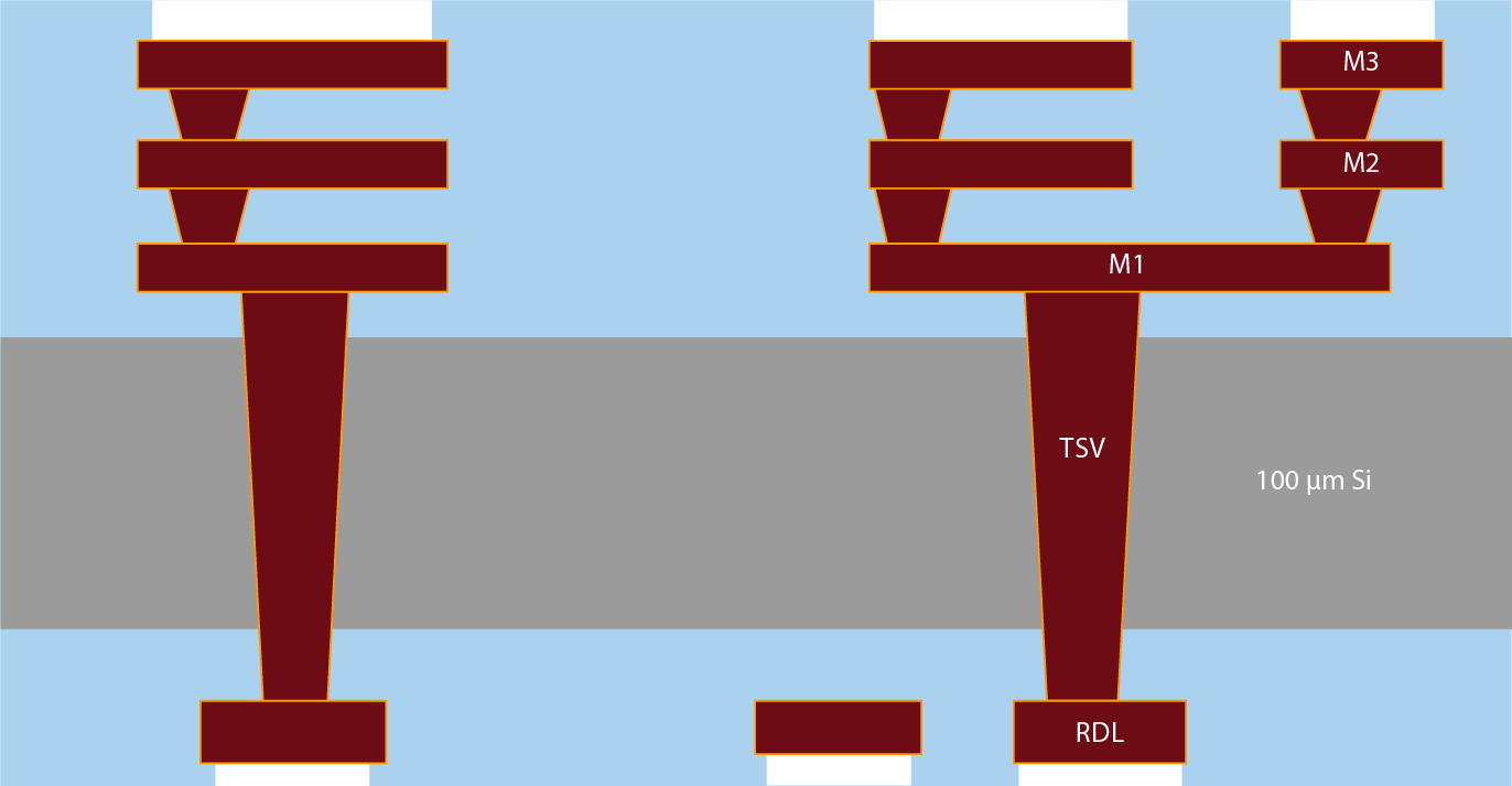
The electronic interposer is a silicon (Si) wafer used for enabling 2.5D integration of photonic and electronic integrated circuits for advanced packaging.
Copper (Cu) lines on the top surface are routed to a backside Cu redistribution layer (RDL) using 10 x 100 µm thru-silicon vias (TSVs). The terminal metal can be bumped (Cu pillar, C2, or C4 solder bumps) for flip-chip packaging.
Advanced packaging operations, such as wafer bumping, flip-chip attach and board assembly, are supported through AIM Photonics Test, Assembly, and Packaging (TAP) facility.
Design Information
AIM Photonics has developed an Electronic Interposer PDK which is supported by the Analog Photonics Electronic Interposer and RF/SUNY Electronic Interposer component libraries. Design rule check is supported in Cadence PVS, Synopsys ICV, and KLayout.
Customization
While we typically follow a standard process flow that designers cannot modify, AIM Photonics has developed a “bite-size” custom offering in which designers can make minor changes to the process flow for an additional fee. This is not a full custom run, and the modification must be something the fab team can execute without additional development work.
Please contact us well in advance of the design due date to ensure that our team understands your request and can properly quote the work.
Customization Options Currently Available for Electronic Interposers
Aluminum termination
Schedule
| Year | Run ID | Design Due Date |
Expected Ship Date |
|---|---|---|---|
| 2024 | EI 24-02E | Jun 3, 2024 | Sep 2, 2024 |
| EI 24-03E | Sep 3, 2024 | Dec 2, 2024 | |
| EI 24-04E | Dec 2, 2024 | Mar 1, 2025 |
Pricing
| Electronic Interposer |
Member (per 20 qty chips) |
Non-Member (per 20 qty chips) |
|---|---|---|
| 156 mm2 | $90,000 | $108,000 |
More Info