
AIM Photonics Introduces Assembly Design Kit to Streamline Photonic Packaging Design
New design tool enables chip-package co-design by embedding packaging considerations in the photonics design workflow
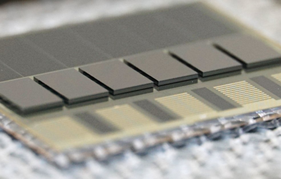
As photonics systems continue to evolve, chip-package co-design is playing an increasingly important role in overall system architecture. By embedding packaging considerations directly into the design workflow, AIM Photonics’ new assembly design kit (ADK) helps bring photonic chip design and assembly processes into closer alignment, enabling more mature prototypes that accelerate the path from design to commercialization.
Packaging challenges have always been a critical part of silicon photonics system design, but packaging requirements have not always been built directly into the design workflow. Instead, designers often rely on guidelines and consultation with packaging teams to ensure compatibility with available processes. However, this collaborative approach can require additional iteration as designs are refined to meet those requirements.
To help bring packaging considerations more directly into the design environment, AIM Photonics has developed its first Assembly Design Kit (ADK). Similar to how a Process Design Kit (PDK) enables designers to create devices compatible with a semiconductor foundry’s manufacturing process, an ADK provides tools and verified components that help ensure photonic integrated circuit (PIC) designs align with available packaging and assembly processes.
“By bringing packaging considerations directly into the design environment, the ADK is expected to help reduce the need for late-stage design changes required to make PIC layouts compatible with AIM Photonics’ assembly and packaging processes,” said Amit Dikshit, AIM Photonics Design Enablement Manager. “Designers can evaluate packaging requirements earlier in the development process using standardized packaging templates and automated design tools, helping reduce design iterations and the likelihood of package re-spins.”
The initial ADK release provides a library of verified components and design templates that help designers align their photonic integrated circuit layouts with AIM Photonics packaging processes. The release supports wirebond and fiber-attach packaging configurations, with templates and verified design data that can be incorporated directly into PIC layouts. Additional features include 3D models, PCB design files and measured data to help designers evaluate packaging considerations during development.
The ADK is currently supported in the KLayout, GDSFactory, Luceda and Cadence design environments and uses parametric cells (P Cells) to help ensure designs remain compatible with packaging requirements.
AIM Photonics ADK also enables multi-physics simulation—including thermal, RF and optical analysis—using verified process parameters, allowing designers to assess packaging considerations as part of the broader system design workflow.
“The combination of verified components, P Cells and simulation capabilities helps designers better understand how their designs will interact with packaging processes,” said Basanth Jagannathan, AIM Photonics Design Enablement Engineer and lead engineer on the ADK. “That level of insight can improve confidence in a design before it reaches assembly.”
Beyond design capabilities, the ADK is expected to improve how customers engage with AIM Photonics’ test, assembly and packaging (TAP) services. By giving designers early visibility into the packaging approaches and processes supported at the TAP facility, the tool allows customers to begin designing with those capabilities in mind rather than developing custom packaging solutions after PIC design is completed. As a result, initial prototypes will arrive at the packaging stage with a higher level of maturity, helping reduce design revisions and enabling more informed discussions with AIM Photonics’ packaging engineers.
“As our assembly and packaging offerings continue to evolve in response to customer needs, a standardized design framework such as the ADK helps align their designs more closely with established assembly processes,” said Chris Striemer, AIM Photonics Director of Test, Assembly and Packaging Operations. “That alignment also simplifies our internal workflows while making it easier for members and customers to design for the capabilities we can support.”
Future ADK releases are expected to expand support for additional packaging approaches, including flip-chip integration, AIM Photonics electronic interposers, photonic wirebonding and microlenses, along with RF board enablement and expanded thermal and RF simulation capabilities. Support for additional EPDA platforms such as Synopsys is also planned, extending the range of design environments supported by the ADK.
Related
Photonics In Focus: Chip-Package Co-Design with AIM Photonics’ Assembly Design Kit (podcast)